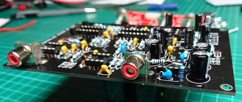
Description
A bare PCB for the MFOS Voltage Controlled analogue reverb unit
- Voltage controlled reverb level
- Voltage controlled original level
Supplied without components or instructions, Soundtronics stock all components needed to build these modules.
Erratum
The official MFOS PCB differs slightly from the instructions / PCB layout on the MFOS website. The VC Reverb was the last product from Ray Wilson before his passing and a few anomalies remain with the PCB. We have identified what we believe are the only differences which are a few components to form a high pass filter R9, R39, R40 & C27. Also C1 and C5 see further down the page.
R40 (100k) is solder on the rear of U1 between pins 3 & 4.

R9 (10k) is soldered to C27 (22nF) before soldering into the R9 position. It is important the resistor and capacitor are soldered exactly as per the photo below. R39 (1k) is soldered from the casing of the phono socket to the junction of R9 and C27.
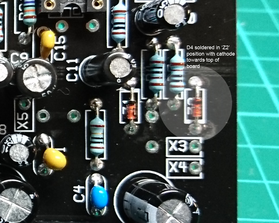
Finally, D4 is shown as Z2 on the PCB silk screen and with an incorrect orientation. Photo below shows D4 in its correct position.
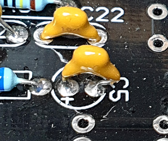
Gary J from Florida also pointed two other differences that we did not mention in the erratum above which relate to C1 and C5.
C1 is a 1uF tantalum capacitor in the schematic and parts list but the PCB silk screen only shows a non-polarised capacitor. C5 on the PCB shows it being polarised but is actually a 100nF non-polarised ceramic capacitor.
When soldering in C1, make sure the +v side of the capacitor is facing towards U1.
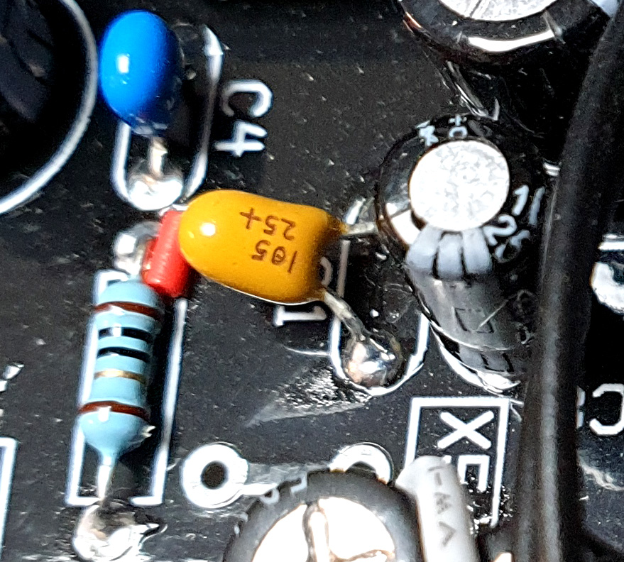
The spacing for C5 is too narrow so simply form the leads to suit, it does not matter which way around it is soldered in.
Supplied without components or instructions. For build instructions see the MFOS website.
Soundtronics (Sonic Synths) MFOS Projects are authorized by Music From Outer Space